- 您现在的位置:买卖IC网 > Sheet目录39245 > LM1262NA/NOPB (NATIONAL SEMICONDUCTOR CORP) 3 CHANNEL, VIDEO PREAMPLIFIER, PDIP24
DAC Interface Register Definitions
(Continued)
DAC 3 Register (I
2C address 06h)
Register name: DAC 3 (06h)
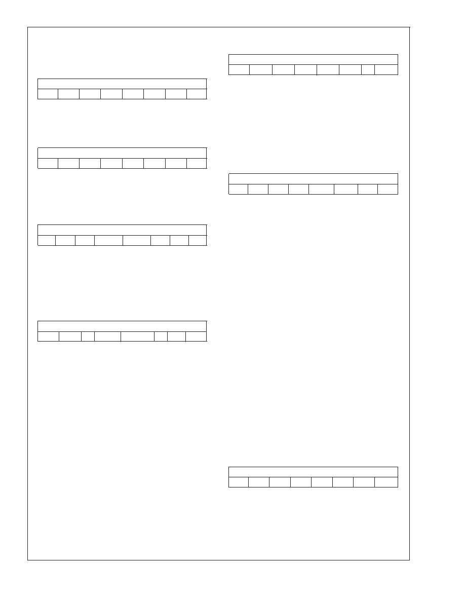
Bit 7
Bit 0
D3–7 D3–6 D3–5 D3–4 D3–3 D3–2 D3–1 D3–0
Bits 7–0: DAC 3. These eight bits determine the output
voltage of DAC 3.
DAC 4 Register (I
2C address 07h)
Register name: DAC 4 (07h)
Bit 7
Bit 0
D4–7 D4–6 D4–5 D4–4 D4–3 D4–2 D4–1 D4–0
Bits 7–0: DAC 4. These eight bits determine the output
voltage of DAC 4.
DC Offset and OSD Contrast Control Register (I
2C ad-
dress 08h)
Register name: DC Offset/OSD Cont. (08h)
Bit 7
Bit 0
RSV
OSDC1
OSDC0
DC2
DC1
DC0
Bits 2–0: DC Offset Control. These three bits determine the
active video DC offset to all three channels.
Bits 4–3: OSD Contrast Control. These two bits determine
the contrast level of the digital OSD information.
Bits 7–5: Reserved.
Global Video Control Register (I
2C address 09h)
Register name: Global Control (09h)
Bit 7
Bit 0
RSV
0
DCF4
DCF1–3
0
PS
BV
Bit 0:
Blank Video. When this bit is a one, blank the
video output. When this bit is a zero allow normal
video out.
Bit 1:
Power Save. When this bit is a one, shut down
the analog circuits to support sleep mode. When
this bit is a zero enable the analog circuits for
normal operation.
Bit 2:
MUST BE SET TO “0” FOR PROPER OPERA-
TION.
Bit 3:
DAC1–3 Configuration. When this bit is a zero
the DAC outputs of DAC1–3 are full scale
(0V–4.5V). When this bit is 1, the range of
DAC1–3 are halved (0V–2.25V).
Bit 4:
DAC4 Configuration. When this bit is a zero the
DAC4 output is not mixed with the other DAC
outputs. When the bit is one, 50% of the DAC4
output is added to DAC1–3.
Bit 5:
MUST BE SET TO “0” FOR PROPER OPERA-
TION.
Bits 7–6: Reserved.
Increment Mode Register (I
2C address 0Ah)
Register name: Increment Mode (0Ah)
Bit 7
Bit 0
RSV
0
INCR
Bit 0:
Increment Enable. When set to a “0”, the default
value, the increment mode is enabled. This al-
lows the registers to be updated sequentially by
sending another block of data.
Bit 1:
MUST BE SET TO “0” FOR PROPER OPERA-
TION.
Bits 7–2: Reserved.
Clamp Polarity, Vertical Blanking, and OSD Control (I
2C
address 0Bh)
Register name: Clamp/VBL/OOR (0Bh)
Bit 7
Bit 0
RSV
CLMP
DAC4
VBL
OOR
Bit 0:
OSD Only Register: When this bit is 0 (default)
normal video operation is assumed. When this bit
is 1, the video is blanked, only the OSD window is
displayed (used for “out-of-range” condition).
Bit 1:
Vertical Blank Enable: When this bit is set to 1 the
vertical blanking pulse is OR’d with the horizontal
blank pulse at the preamplifier output, to blank
the video during both the vertical and horizontal
retrace. I
2C changes for contrast and DAC4 will
only be updated during vertical retrace period.
When this bit is set to 0 (default) the internal
vertical blanking is disabled (horizontal blanking
is not affected) and I
2C changes for contrast and
DAC4 occur anytime in the video field. NOTE: If
there is no vertical signal to the LM1262, this bit
must be set to a 0 for proper operation.
Bit 2:
DAC4 I/O Switch: When this bit is set to 1 (de-
fault) DAC4 output is enabled. When this bit is set
to a 0 the DAC4 output is disabled and pin 13 is
used for the vertical blank input. DAC4 can still be
connected internally to DAC1-3. When both bits 1
and 2 are set to 1 vertical blanking will be stripped
from the sandcastle pulse at pin 23. For proper
detection of the sandcastle pulse the CLMP bit
(bit 3) must be set to a 0, positive polarity for the
clamp input.
Bit 3:
Determines the polarity of the clamp signal used
by the LM1262, “0” (default) is a positive clamp
signal, “1” is a negative going clamp signal.
Bits 7–4: Reserved.
Software Reset Register (I2C address 0Fh)
Register name: Software Reset (0Fh)
Bit 7
Bit 0
RSV
SRST
Bit 0:
Software Reset. Setting this bit causes a software
reset. All registers (except this one) are loaded
with their default values. All operations currently
in progress are aborted (except for I
2C transac-
tions). This bit automatically clears itself when the
reset has been completed.
Bits 7–1: Reserved.
LM1262
www.national.com
19
发布紧急采购,3分钟左右您将得到回复。
相关PDF资料
LM129BH/883
1-OUTPUT TWO TERM VOLTAGE REFERENCE, 6.9 V, MBCY2
LM129BH
1-OUTPUT TWO TERM VOLTAGE REFERENCE, 6.9 V, MBCY2
LM12H454CIV
SPECIALTY ANALOG CIRCUIT, PQCC44
5962-9319501MXC
SPECIALTY ANALOG CIRCUIT
5962-9319502MYX
SPECIALTY ANALOG CIRCUIT, PQCC44
5962-9319501MYX
SPECIALTY ANALOG CIRCUIT, PQCC44
5962-9319501MXX
SPECIALTY ANALOG CIRCUIT
5962-9319502MXX
SPECIALTY ANALOG CIRCUIT, CQCC44
相关代理商/技术参数
LM1267
制造商:NSC 制造商全称:National Semiconductor 功能描述:150 MHz I2C Compatible RGB Video Amplifier System with OSD and DACs
LM1267NA
制造商:NSC 制造商全称:National Semiconductor 功能描述:150 MHz I2C Compatible RGB Video Amplifier System with OSD and DACs
LM1267NA/NOPB
功能描述:IC PREAMP RGB 150MHZ 24-DIP RoHS:是 类别:集成电路 (IC) >> 线性 - 视频处理 系列:- 产品变化通告:Product Discontinuation 07/Mar/2011 标准包装:3,000 系列:OMNITUNE™ 类型:调谐器 应用:移动电话,手机,视频显示器 安装类型:表面贴装 封装/外壳:65-WFBGA 供应商设备封装:PG-WFSGA-65 包装:带卷 (TR) 其它名称:SP000365064
LM1269
制造商:NSC 制造商全称:National Semiconductor 功能描述:110 MHz I2C Compatible RGB Video Amplifier System with OSD & DACs
LM1269DNA
制造商:Texas Instruments 功能描述:
LM1269DNA/NOPB
功能描述:IC PREAMP CMOS 110MHZ 24-DIP RoHS:是 类别:集成电路 (IC) >> 线性 - 视频处理 系列:- 产品变化通告:Product Discontinuation 07/Mar/2011 标准包装:3,000 系列:OMNITUNE™ 类型:调谐器 应用:移动电话,手机,视频显示器 安装类型:表面贴装 封装/外壳:65-WFBGA 供应商设备封装:PG-WFSGA-65 包装:带卷 (TR) 其它名称:SP000365064
LM1269NA
制造商:Texas Instruments 功能描述:Video Amplifiers 制造商:Texas Instruments 功能描述:-LIFETIME BUYS TIL 05/12
LM1269NA/NOPB
功能描述:视频放大器 RoHS:否 制造商:ON Semiconductor 通道数量:4 电源类型: 工作电源电压:3.3 V, 5 V 电源电流: 最小工作温度: 最大工作温度: 封装 / 箱体:TSSOP-14 封装:Reel